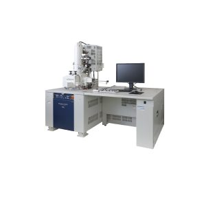
The Hitachi SU9000 Ultrahigh-Resolution Scanning Electron Microscope (SEM) is a premium SEM that sets a new standard in ultrahigh-resolution imaging and advanced technology. Top-of-the-line in lens FE-SEM (Field-Emission Scanning Electron Microscope that brings together Hitachi’s total technical capabilities. Moreover, it enables observation of lattice images of graphite with 0.34 nm resolution (30 kV/STEM). Ultimately, this is Hitachi’s highest performance FE-SEM, supporting cutting edge research and development.
Features of Hitachi SU9000 Ultra-High-Resolution SEM
World’s Highest SE Resolution
Achieves an SE resolution of 0.4 nm at 30 kV, ensuring unparalleled image clarity.
Exceptional Magnification
Offers usable magnification up to 3,000,000x, allowing for detailed examination of specimens.
Advanced CFE Gun
The newly designed cold field emission (CFE) gun provides high brightness and an extremely stable emission current.
Superior Low kV Performance
Ideal for observing beam-sensitive materials with superior low kV performance.
Next-Generation In-Lens SEM Optics
Allows for routine observation at 1,000,000x magnification.
Improved Vacuum Technology
Achieves ultra-high vacuum (UHV) levels to reduce sample contamination.
Robust Instrument Enclosure
Features superior strength and stability for high-resolution imaging in various environmental conditions.
Innovative Objective Lens
Enables high-resolution imaging at low acceleration voltages.
Efficient Sample Exchange System
The side entry sample exchange system increases throughput by reducing the time required to change samples and automatically positioning the sample at the current working distance (WD).
The Hitachi SU9000 Ultrahigh-Resolution SEM is designed to meet the rigorous demands of advanced research and industrial applications. With its unmatched resolution, exceptional magnification, and advanced features, this SEM provides precise and efficient observation of specimens, making it an invaluable tool for scientists and engineers.
Application
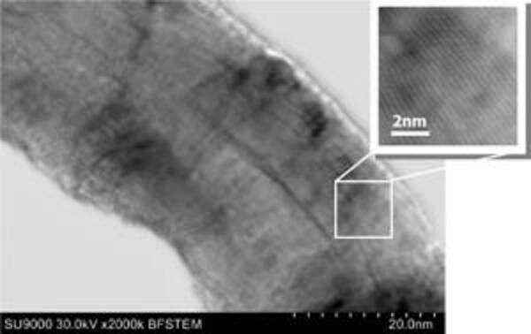
Sample : Multi wall carbon nano tube (lattice fringes)
Vacc : 30 kV
Mag. : 2,000kx
Bright Field(BF)-STEM image


