Mechanical Cross-Sectioning
Sample preparation of cross sections can be performed with an assortment of instruments and methods, and the process necessitates a different equipment setup, depending on the level of automation. For the preparation of simple SEM cross sections of IC devices, there are essentially two approaches that are possible among the established practices: encapsulated cross sections and un-encapsulated cross sections.
Encapsulated Cross-Section: Encapsulated cross-section methods commence by mounting a cross-sectional sample into an epoxy or acrylic mold compound, conventionally around 1 inch in diameter, and surrounding the selected device, to ensure the sample is simpler to handle.
The mold is then ground and polished until the cross section is finished. In general, the procedure requires silicon carbide abrasive papers from 120 to 1200 grit, and ultimately concludes with a final polish undertaken with 0.05 μm colloidal silica administered to a polishing cloth.
The mold is then ground and polished until the cross section is finished. In general, the procedure requires silicon carbide abrasive papers from 120 to 1200 grit, and ultimately concludes with a final polish undertaken with 0.05 μm colloidal silica administered to a polishing cloth.
Un-Encapsulated Cross-Section:
Un-encapsulated cross sectioning is executed directly on the desired IC device. The sample is incised to appropriate proportions (typically around 3 x 5mm) and affixed to a variety of holder. The sample is subsequently polished with the use of diamond lapping films of 30 μm – 0.5 μm, and ultimately concludes with a final polish undertaken with 0.05 μm colloidal silica administered to a polishing cloth.
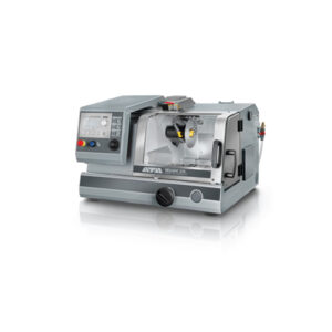
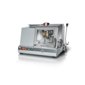
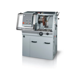
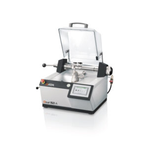
The equipment configuration has to diverge to enable the implementation of either approach. Each technique necessitates a variety of polishing machine to grind and polish the sample down to the appropriate surface finish needed for scanning electron microscope examination.

